Modules#
Modules connect to a simple single-master bus. Every module has a similar set of parameters and pins for bus integration. The full list of firmware modules can be found in the firmware/modules folder, and their Python drivers in basil/HL.
The following parameters, pins, and registers are common to all bus-connected modules. Individual modules add their own on top of these.
Common parameters:
Name |
Default |
Description |
|---|---|---|
BASEADDR |
0 |
Defines base address of module (start address) in memory map space |
HIGHADDR |
0 |
Defines last module address in memory map space |
ABUSWIDTH |
16 |
Address bus width |
DBUSWIDTH |
8 |
Data bus width |
Common pins:
Name |
Size |
Direction |
Description |
|---|---|---|---|
BUS_RST |
1 |
input |
Synchronous reset, active high |
BUS_CLK |
1 |
input |
Bus clock |
BUS_WR |
1 |
input |
Write strobe, active high |
BUS_RD |
1 |
input |
Read strobe, active high |
BUS_ADD |
ABUSWIDTH |
input |
Address bus |
BUS_DATA |
DBUSWIDTH |
inout |
Data bus |
Common registers:
Name |
Address |
r/w |
Description |
|---|---|---|---|
RESET |
0 |
wo |
Soft reset on write to address |
VERSION |
0 |
ro |
Module version |
gpio - General purpose IO#
General purpose input output (gpio) is a generic pins whose behavior, including whether it is an input or output pin, can be controlled by the user at run time.
Unit test/Example: test_SimGpio.v test_SimGpio.py
Usage notes
StdRegister usage: Rather than reading/writing the raw INPUT and OUTPUT bytes directly, instantiate a
StdRegisterin the basil configuration YAML with named fields for each GPIO bit. This provides access likedaq["gpio0"]["RST_B"] = 1followed by .write() to push the full byte to hardware.Direction: Each pin’s direction is set by IO_DIRECTION at compile time. Runtime direction changes via the DIRECTION register require IO_TRI to be enabled for the corresponding pin.
- Parameters:
Name
Default
Description
IO_WIDTH
8
Defines io width in bits
IO_DIRECTION
0
Defines direction for every pin separate, 0 - input, 1 - output
IO_TRI
0
instantiate tri-state buffer for given pin
- Pins:
Name
Size
Direction | Description
IO
IO_WIDTH
IO_DIRECTION/IO_TRI | General purpose pins
- Registers:
Name
Address
Description
RESET
0
Soft reset active on write to address
INPUT
1 to BYTE
Readback of state of pin
OUTPUT
1+BYTE to 2*BYTE
Set output state on pin
DIRECTION
1+2*BYTE to 3*BYTE
Tri-state pin (if enabled)
Where: BYTE = IO_WIDTH/8+1
Driver:
GPIO hardware layer for Basil.
- class basil.HL.gpio.gpio(intf, conf)[source]#
GPIO interface.
- get_data()[source]#
Read the GPIO INPUT register. Returns the current logic levels on all pins as a byte array. Reads the physical pin state regardless of direction configuration.
- get_output_en()[source]#
Return the output enable mask. Each bit indicates whether the corresponding pin is in output mode (1) or input mode (0).
spi - Serial peripheral interface#
Module implements master serial peripheral interface. Supports simple internal loops.
Unit test/Example: test_SimSpi.v test_SimSpi.py
Usage notes
External start: When
ENis set, the SPI transfer can be triggered via theEXT_STARTpin instead of a software write toSTART.Repeat mode: A value of 0 in the
REPEATregister causes the transfer to repeat forever.START and DONE share the same address: The
START(write-only) andDONE(read-only) registers are aliased at the same address. Writing to address 1 triggers a start, reading address 1 returns the done flag. This pattern is consistent across seq_gen, spi, and pulse_gen.
- Parameters:
Name
Default
Description
MEM_BYTES
16
Amount of memory allocated for data (maximum single transfer in bytes)
- Pins:
Name
Size
Direction
Description
SPI_CLK
1
input
clock used for SPI transfers
SCLK
1
output
external clock (active only during transfers)
SDO
1
input
incoming data
SDI
1
output
outgoing data
SEN
1
output
active high during transfer
SLD
1
output
active high strobe indicating end of transfer
EXT_START
1
input
active high start signal (synchronous to SPI_CLK)
- Registers:
Name
Address
Bits
r/w
Default
Description
START / DONE
1
wo/ro
0
Start transfer / Indicate transfer finish
SIZE
4 - 3
[15:0]
r/w
MEM_BYTES*8
Set the size of transfer in bits
WAIT
8 - 5
[31:0]
r/w
4
Waits after every transfer if REPEAT != 0
REPEAT
12 - 9
[31:0]
r/w
1
Repeat transfer count (0 -> forever)
EN
13
[0]
r/w
0
Enable external start (0 -> soft start only)
MEM_BYTES
15 - 14
[15:0]
ro
MEM_BYTES
Byte size of memory
DATA_OUT
16 to 16+MEM_BYTES-1
r/w
unknown
Memory for outgoing data
DATA_IN
16+MEM_BYTES to 16+2*MEM_BYTES-1
r/w
unknown
Memory for incoming data
Driver:
Serial programming interface (SPI) driver for FPGA-based SPI modules.
- class basil.HL.spi.spi(intf, conf)[source]#
Implement serial programming interface (SPI) driver.
- get_data(size=None, addr=None)[source]#
Read data from the SPI receive memory at the bus memory offset.
Incoming bytes captured from SDO are stored here.
- Args:
size (int, optional): Number of bytes to read (default all). addr (int, optional): Byte offset into memory.
- get_mem_size()[source]#
Return the SPI memory size in bytes (from MEM_BYTES register at address 14-15). This is the maximum single transfer size.
- get_repeat()[source]#
Get number of repetitions of sequence with delay ‘wait’ (if 0 –> repeat forever).
- is_done()[source]#
Return True if the SPI transfer is complete, False if still in progress.
Aliases is_ready.
- property is_ready#
Read the DONE/READY register at address 1. Returns True when the transfer is complete, False while shifting.
- set_data(data, addr=0)[source]#
Write data to the SPI transmit memory at the bus memory offset.
Data bytes are shifted out MSB-first on SDI.
- Args:
data (bytes): Data to write. addr (int, optional): Byte offset into memory.
- set_en(value)[source]#
Enable start on external EXT_START signal (inside FPGA).
When enabled, the SPI transfer starts on the external EXT_START signal.
- set_repeat(value)[source]#
Set the number of repetitions of the sequence with delay ‘wait’.
If 0: Repeat sequence forever. Otherwise: Number of repetitions of sequence with delay ‘wait’.
- set_size(value)[source]#
Set the number of clock cycles for shifting in data.
For example, length of matrix shift register (number of pixels daisy chained).
seq_gen - Pattern generator#
Module implements a simple sequencer/pattern generator based on block ram. Supports 2 levels of internal loops and external start.
Unit test/Example: test_SimSeq.v test_SimSeq.py
Usage notes
Tracks: The seq_gen supports OUT_BITS from 1 to at least 256. Each output bit is a separate track. To fill track data in software, instantiate a
TrackRegisterin the basil configuration YAML. This provides named track access likedaq["seq0"]["INIT"][0:40] = bitarray("...").Start: The sequence can be started via a write to the
STARTregister (software start), or via the SEQ_EXT_START pin withEN_EXT_STARTset (external start). The external start is typically driven by a GPIO or pulse_gen output.Repeat mode: A value of 0 in the
REPEATregister causes the sequence to repeat forever (until reset or reconfiguration).Output hold: When the sequence finishes or stops, the last output state is held on
SEQ_OUT— it does not return to zero. The sequencer does not reset its outputs on completion.START and READY share the same address: The
START(write-only) andDONE(read-only) registers are aliased at the same address. Writing to address 1 triggers a start, reading address 1 returns the done flag. This pattern is consistent across seq_gen, spi, and pulse_gen.
- Parameters:
Name
Default
Description
MEM_BYTES
16384
Amount of memory allocated for data (in bytes)
OUT_BITS
8
Size (bit) for output pattern - word size
- Pins:
Name
Size
Direction
Description
SEQ_EXT_START
1
input
external start signal (synchronous to SEQ_CLK)
SEQ_CLK
1
input
external clock used for driving sequence
SEQ_OUT
OUT_BITS
output
sequencer output
- Registers:
Name
Address
Bits
r/w
Default
Description
RESET / VERSION
0
wo/ro
Soft reset on write / Firmware version
START / DONE
1
wo/ro
0
Start sequence on write / Indicates sequence finished
EN_EXT_START
2
[0]
r/w
0
Enable external start
CLK_DIV
3
[7:0]
r/w
1
Internal division factor for SEQ_CLK
SIZE
7 - 4
[31:0]
r/w
out_words
Set the size of sequence (in output words)
WAIT
11 - 8
[31:0]
r/w
0
Waits after every sequence if REPEAT != 0 (0 -> forever)
REPEAT
15 - 12
[31:0]
r/w
1
Repeat sequence count (0 -> forever)
REP_START
19 - 16
[31:0]
r/w
0
Position from which pattern will start in repeat mode (first sequence always starts at 0)
NESTED_START
23 - 20
[31:0]
r/w
0
Position from which pattern will start for nested loop
NESTED_STOP
27 - 24
[31:0]
r/w
0
Position to which pattern will stop for nested loop
NESTED_REPEAT
31 - 28
[31:0]
r/w
0
Repeat count for nested loop
MEM_BYTES
35 - 32
[31:0]
ro
MEM_BYTES
Memory size (read only)
DATA
64 to 64+MEM_BYTES-1
r/w
unknown
Memory for pattern
Driver:
Sequence generator driver for the seq_gen FPGA module.
- class basil.HL.seq_gen.seq_gen(intf, conf)[source]#
Sequence generator controller interface for seq_gen FPGA module.
- get_data(size=None, addr=0)[source]#
Read sequencer memory (the pattern data) via the bus interface.
- Args:
size: Number of bytes to read (default: all). addr: Optional byte offset into memory.
- Returns:
bytes: The pattern data.
- is_done()[source]#
Return True if the sequencer has finished its sequence.
Includes all repeats. Returns False while running. Aliases is_ready.
- property is_ready#
Read the DONE/READY register (addr 1, bit 0).
Returns True when the sequencer is idle and ready to accept a new start trigger. While the sequence is running (including all configured repetitions) this reads False.
The
@propertydecorator makes this an attribute-like access — call it without parentheses asdaq["seq0"].is_ready, not.is_ready()..is_done()and.get_done()are aliases that return the same value.
- reset()[source]#
Soft reset the sequencer.
Clears internal counters and output state on the next clock edge. Must have a rising edge on the sequencer clock before new data is written to memory.
- set_clk_divide(value)[source]#
Set the clock division factor for SEQ_CLK.
The sequencer advances one step every CLK_DIV + 1 clock cycles. Default: 1 (divide by 1, i.e. full rate). Address 3.
- set_data(data, addr=0)[source]#
Write sequencer memory (the pattern data) via the bus interface.
Data is interleaved per track by the TrackRegister RL.
- Args:
data: Bytes to write to sequencer memory. addr: Optional byte offset into memory.
- set_en_ext_start(value)[source]#
Enable or disable external start via the SEQ_EXT_START pin.
When enabled (1), the SEQ_EXT_START pin rising edge triggers the sequence. When disabled (0), only software .start() works. Address 2.
- set_repeat(value)[source]#
Set the repeat count.
0 = repeat forever. The sequence repeats from REP_START (or 0) each time. Addresses 12-15.
- set_repeat_start(value)[source]#
Set the repeat start position.
When repeating, the sequence jumps to this position instead of starting from 0. Addresses 16-19.
- set_size(value)[source]#
Set the number of output words in the sequence.
Each word contains OUT_BITS (one sample per track). Addresses 4-7.
pulse_gen - Pulse generator#
Simple pulse generator with configurable delay and width.
Unit test/Example: test_SimSeq.v test_SimSeq.py
Usage notes
Start: The pulse can be started via a write to the
STARTregister (software start), or via theEXT_STARTpin withENset (external start).Repeat mode: A value of 0 in the
REPEATregister causes the pulse to repeat forever.START and READY share the same address: The
START(write-only) andREADY(read-only) registers are aliased at the same address. Writing to address 1 triggers a start, reading address 1 returns the ready flag. This pattern is consistent across seq_gen, spi, and pulse_gen.
- Pins:
Name
Size
Direction
Description
EXT_START
1
input
active high start signal (synchronous to PULSE_CLK)
PULSE_CLK
1
input
module clock
PULSE
1
output
output pulse
- Registers:
Name
Address
Bits
r/w
Default
Description
RESET / VERSION
0
wo/ro
Soft reset on write / Firmware version
START / READY
1
wo/ro
0
Software start on write / Indicate finish
EN
2
[0]
r/w
0
Enable external start
DELAY
6 - 3
[31:0]
r/w
0
Pulse delay from start
WIDTH
10 - 7
[31:0]
r/w
0
Pulse width
REPEAT
14 - 11
[31:0]
r/w
1
Repeat count (0 -> forever)
Driver:
Register-based interface to the pulse_gen hardware block.
- class basil.HL.pulse_gen.pulse_gen(intf, conf)[source]#
Pulse generator.
- get_en()[source]#
Return whether the pulse uses a fixed delay w.r.t. the shift register finish signal.
- is_done()[source]#
Return True if the pulse generator has finished all repetitions, False if still active. Alias of is_ready.
- property is_ready#
Return True when the pulse generator is idle and ready to accept a new start trigger.
Reads the READY register (addr 1, bit 0). While the pulse is running (including all configured repetitions) this reads False.
The @property decorator makes this an attribute-like access - call it without parentheses as
daq["pulse0"].is_ready, not.is_ready()..is_done() is an alias that returns the same value.
- set_delay(value)[source]#
Set the pulse delay in clock cycles from start.
The delay is relative to the start trigger (software .start() or EXT_START pin).
- set_en(value)[source]#
Configure whether the pulse synchronizes with an external trigger.
If true: The pulse comes with a fixed delay with respect to the external trigger (EXT_START). If false: The pulse comes only at software start.
rrp_arbiter - Round-robin arbiter#
Round-robin arbiter for data (32 bit) streams with priority. Data streams multiplexer.
- Parameters:
Name
Default
Description
WIDTH
4
Number of incoming data streams
- Pins:
Name
Size
Direction
Description
WRITE_REQ
WIDTH
input
indicate will of writing data
HOLD_REQ
WIDTH
input
wait for writing for given stream (priority)
DATA_IN
WIDTH*32
input
incoming data for arbitration
READ_GRANT
WIDTH
output
indicate to stream that data has been accepted
READY_OUT
1
input
indicate ready for outgoing stream
WRITE_OUT
1
output
indicate will of write to outgoing stream
DATA_OUT
32
output
outgoing data stream
No Python driver — this module operates autonomously in the FPGA fabric.
seq_rec - Data recorder#
Simple module that allow recording arbitrary data vector.
Unit test/Example: test_SimSeq.v test_SimSeq.py
Driver:
cmd_seq - Command generator (FE-I4)#
Generate arbitrary single bit data stream and clock (mainly to generate FE-I4 commands). Supports hardware loops and Manchester data encoding.
Driver:
fei4_rx - FE-I4 data receiver#
Allows continuous data recording from FE-I4. Received data are propagated to FIFO data interface. Implements auto synchronization and data error monitoring.
Driver:
fast_spi_rx - Fast serial receiver#
This module can continuous capture serial data on each rising edge of it’s capture clock. Received data is packed into 32-bit words and propagated to a FIFO data interface. While originally intended for SPI (hence the naming), it can be used for any serial data.
Unit tests
Unit tests for this module have not yet been implemented.
Usage notes
Data output format: Each 32-bit FIFO word is formatted as
[31:28] IDENTIFIER, [27:N] Frame counter, [N-1:0] Captured datawhereN = DATA_SIZE. The IDENTIFIER field differentiates multiple fast_spi_rx instances merged into the same downstream FIFO stream. The frame counter increments on every SEN falling edge, allowing reconstruction of multi-word captures. When a capture spans multiple FIFO words, all words carry the same frame counter value.FIFO flush behavior: A FIFO word is written when DATA_SIZE bits have been captured, or when SEN falls (flushing any partially-filled word). An incomplete frame is never lost — it is always written to the FIFO when SEN goes low.
Reset: The soft reset (RESET register write or BUS_RST) is synchronised to SEQ_CLK via a CDC synchroniser. At least one rising edge of SEQ_CLK must occur after reset is released for it to take effect. If SEQ_CLK is not running when reset is asserted, the reset will not complete.
Parameters#
Name
Default
Description
ABUSWIDTH
16
Width of the bus address bus
IDENTIFIER
4’b0001
Instance identifier packed into bits [31:28] of each FIFO word
DATA_SIZE
16
Number of serial data bits packed into a single FIFO word
Pins#
Name
Size
Direction
Description
SEQ_CLK
1
input
Capture clock (serial data sampled on rising edge)
SDI
1
input
Serial data input (sampled on SEQ_CLK rising edge)
SEN
1
input
Serial enable (active high, frames the capture)
FIFO_READ
1
input
Read strobe (pop one word from the output FIFO)
FIFO_EMPTY
1
output
FIFO empty flag
FIFO_DATA
32
output
FIFO data output (32-bit word)
Registers#
Name
Address
Bits
r/w
Default
Description
RESET
0
wo
Soft reset (synchronous to SEQ_CLK, takes effect on next edge)
VERSION
0
[7:0]
ro
Firmware version
EN
2
[0]
r/w
0
Enable capture (set high to arm)
LOST_COUNT
3
[7:0]
ro
0
Lost data counter (incremented on CDC FIFO overflow)
Unit tests
Unit tests for this module have not yet been implemented.
Driver:
Fast SPI receive interface for reading variable-width serial data.
Provides a register-level hardware layer to arm/disarm capture, query frame-size configuration, check for lost words, and parse 32-bit FIFO words into (identifier, frame_counter, spi_data) tuples.
- class basil.HL.fast_spi_rx.fast_spi_rx(intf, conf)[source]#
Fast SPI interface with variable data width support.
The module outputs 32-bit words containing: - IDENTIFIER (4 bits) - Frame counter (28 - DATA_SIZE bits) - SPI data (DATA_SIZE bits)
The DATA_SIZE parameter must match the DATA_SIZE parameter used in the FPGA firmware (fast_spi_rx_core.v).
Captured data is read via the dedicated FIFO output ports (not the register bus). At the system level, these feed into a SiTCP FIFO stream accessed through daq[“fifo0”].get_data().
- get_lost_count()[source]#
Return the count of lost data words due to CDC FIFO overflow.
Non-zero indicates the capture rate exceeded the readout rate.
- get_size()[source]#
Return the DATA_SIZE (SPI data width in bits) used for parsing captured words.
Reads the value from the hardware DATA_SIZE register (addr 4).
- parse_word(word)[source]#
Parse a 32-bit FIFO word into (identifier, frame_counter, spi_data).
The split between frame counter and captured data is determined by get_size(). Useful for parsing words read via daq[“fifo0”].get_data().
- Args:
word: A 32-bit integer from the fast_spi_rx output FIFO.
- Returns:
tuple: (identifier, frame_counter, spi_data)
tlu - Trigger logic unit#
General purpose trigger module and EUDAQ Telescope/TLU communication module. Trigger IDs received by the TLU are propagated to FIFO data interface.
- NOTE:
TRIGGER_ENABLE register has to be set to true to enable trigger FSM.
EXT_TRIGGER_ENABLE and TRIGGER_ACKNOWLEDGE input signals needs to be synchronous to TRIGGER_CLOCK.
Data words have the MSB always high to allow identification of trigger data words. The remaining 31 bits are data.
All selected trigger inputs are ORed. Trigger inputs are connected to TRIGGER input. Trgger inputs are selected by applying a bit mask to TRIGGER_SELECT.
All selected veto inputs are ORed. Veto inputs are connected to TRIGGER_VETO input. Veto inputs are selected by applying a bit mask to TRIGGER_VETO_SELECT.
If TRIGGER_LOW_TIMEOUT_ERROR_COUNTER in TLU handshake mode is not 0, the busy signal might be broken.
If TLU_TRIGGER_ACCEPT_ERROR_COUNTER in TLU handshake mode is not 0, the TLU might be not configured properly (must be in handshake mode) or short pulses are appearing on the trigger line. Possible solution is to increase TRIGGER_HANDSHAKE_ACCEPT_WAIT_CYCLES.
TLU_TRIGGER_MAX_CLOCK_CYCLES should always be one more clock cycle than the bit lenght of the trigger data to return the trigger line to logical low.
- TRIGGER_MODE[1:0]:
0 = normal trigger mode (receiving triggers from input TRIGGER)
1 = EUDAQ TLU - no handshake
2 = EUDAQ TLU - simple handshake
3 = EUDAQ TLU - trigger data handshake
- DATA_FORMAT[1:0]:
0 = trigger number according to TRIGGER_MODE
1 = time stamp only
2 = combined, 15bit time stamp + 16bit trigger number
3 = n/a
Unit test/Example: test_SimTlu.v test_SimTlu.py
- Parameters:
Name
Default
Description
DIVISOR
8
Defines TLU clock speed. TLU clock is divided by Divisor.
TLU_TRIGGER_MAX_CLOCK_CYCLES
17
Number of clock cycles send to the TLU. Bit lenght of trigger data is -1.
WIDTH
8 (max. 32)
Bus width of the trigger input and trigger veto input.
TIMESTAMP_N_OF_BIT
32
Bus width of time stamp.
- Pins:
Name
Size
Direction
Description
TRIGGER_CLK
1
input
clock for module
TRIGGER_ENABLED
1
output (sync)
assert signal when trigger FSM is enabled and running
TRIGGER_SELECTED
WIDTH (max. 32)
output (sync)
selected trigger inputs
TLU_ENABLED
1
output (sync)
assert signal when trigger mode is != 0 (EUDAQ TLU)
TRIGGER
WIDTH (max. 32)
input (async)
extenel trigger (see also WIDTH parameter)
TRIGGER_VETO
WIDTH (max. 32)
input (async)
external veto (see also WIDTH parameter)
TIMESTAMP_RESET
1
input (async)
resetting timestamp counter
EXT_TRIGGER_ENABLE
1
input (sync)
enables sync with other external devices/modules
TRIGGER_ACKNOWLEDGE
1
input (sync)
signal/flag from external devices/modules if ready
TRIGGER_ACCEPTED_FLAG
1
output
flag if trigger is valid and was accepted
FIFO_PREEMPT_REQ
1
output
fast signal that put arbiter on hold
TLU_TRIGGER
1
input (async)
TLU trigger input
TLU_RESET
1
input (async)
TLU reset input
TLU_BUSY
1
output
TLU busy output
TLU_CLOCK
1
output
TLU clock output
EXT_TIMESTAMP
TIMESTAMP_N_OF_BIT
input (sync)
timestamp from external source (optional)
TIMESTAMP
TIMESTAMP_N_OF_BIT
output (sync)
internal timestamp provided for other devices/modules
- Registers:
Name
Address
Bits
r/w
Default
Description
RESET
0
wo
reset
VERSION
0
[7:0]
ro
0
version
TRIGGER_MODE
1
[1:0]
r/w
0
external/TLU trigger mode
TRIGGER_DATA_MSB_FIRST
1
[2]
r/w
0
TLU trigger number MSB
TRIGGER_ENABLE
1
[3]
r/w
0
enable trigger FSM
USE_EXT_TIMESTAMP
1
[4]
r/w
0
use timestamp from EXT_TIMESTAMP input
DATA_FORMAT
2
[1:0]
r/w
0
format of trigger number output
EN_TLU_RESET_TIMESTAMP
2
[5]
r/w
0
reset time stamp to 0 on TLU reset (handsh. mode only)
EN_TLU_VETO
2
[6]
r/w
0
assert TLU veto when external veto
TRIGGER_LOW_TIMEOUT
3
[7:0]
r/w
255
max. wait cycles for TLU trigger low (0=off)
CURRENT_TLU_TRIGGER_NUMBER
7 - 4
[31:0]
ro
last TLU trigger number
TRIGGER_COUNTER
11 - 8
[31:0]
r/w
0
trigger counter value
LOST_DATA_COUNTER
12
[7:0]
ro
lost data counter
TRIGGER_SELECT
13 - 16
[31:0]
r/w
0
selecting trigger input (see also WIDTH parameter)
TRIGGER_VETO_SELECT
17 - 20
[31:0]
r/w
0
selecting veto input (see also WIDTH parameter)
TRIGGER_INVERT
21 - 24
[31:0]
r/w
0
inverting selected trigger input
MAX_TRIGGERS
25 - 28
[31:0]
r/w
0
maximum triggers, use 0 for unltd. triggers
TRIGGER_HANDSHAKE_ACCEPT_WAIT_CYCLES
29
[7:0]
r/w
3
TLU trigger minimum length in TLU clock cycles
HANDSHAKE_BUSY_VETO_WAIT_CYCLES
30
[7:0]
r/w
0
additional wait cycles before de-asserting TLU busy
TRIGGER_LOW_TIMEOUT_ERROR_COUNTER
31
[7:0]
ro
trigger low timeout error counter
TLU_TRIGGER_ACCEPT_ERROR_COUNTER
32
[7:0]
ro
trigger accept error counter
TRIGGER_THRESHOLD
33
[7:0]
r/w
0
trigger minimum length in TLU clock cycles
SOFT_TRIGGER
34
[7:0]
wo
n/a
manual software trigger (requires TRIGGER_MODE=0)
TRIGGER_DATA_DELAY
35
[7:0]
r/w
0
additional TLU data delay for longer cables
Driver:
tdc - Time-to-digital converter#
Simple time to digital converter. This module digitizes (12 bit resolution) input pulse (TDC_IN) and calculates distance (8 bit resolution) between TDC_IN and TRIG_IN (e.g. trigger signal and hit). Calculated values (see data format, always 32-bit) are propagated to FIFO data interface.
- NOTE:
Use BROADCAST parameter in order to share fast (640 MHz sampled) trigger signal with other tdc modules.
TDC_IN needs to be longer than one cycle of CLK320, distance of TDC_IN and TRIG_IN needs to be longer than one clock cycle of DV_CLK.
TRIG_IN needs to come before (at least one clock cycle of DV_CLK) TDC_IN.
ARM_TDC and EXT_EN are assumed to be slower than DV_CLK.
Unit test/Example: test_SimTdc.v test_SimTdc.py
- Data format (Standard)
DATA IDENTIFIER (4 bit)
EVENT_COUNTER (16 bit)
TDC value (12 bit)
- Data format (in case of EN_WRITE_TIMESTAMP)
DATA IDENTIFIER (4 bit)
TIMESTAMP (16 bit)
TDC value (12 bit)
- Data format (in case of EN_TRIGGER_DIST)
DATA IDENTIFIER (4 bit)
TRIGGER DIST (8 bit)
TIMESTAMP/EVENT COUNTER (8 bit)
TDC value (12 bit)
- Parameters:
Name
Default
Description
CLKDV
4 (min. 2)
Factor of CLK160 to DV_CLK, minimal divider of 2.
DATA_IDENTIFIER
4’b0100
4-bit data identifier for TDC words.
FAST_TDC
1
If FAST_TDC is 1, 640 MHz sampling of input TDC_IN is done, else 320 MHz sampling is done.
FAST_TRIGGER
1
If FAST_TRIGGER is 1, 640 MHz sampling of input TRIG_IN is done, else 320 MHz sampling is done.
BROADCAST
0
If BROADCAST is 1, 640 MHz sampled trigger signal can be shared with other TDC modules.
- Pins:
Name
Size
Direction
Description
CLK320
1
input
320 MHz clock
CLK160
1
input
160 MHz clock
DV_CLK
1
input
clock for ?
TDC_IN
1
input
input pulse which is digitized
TDC_OUT
1
ouput
output TDC pulse
TRIG_IN
1
input
input trigger signal (distance between TRIG_IN and TDC_IN is calculated)
TRIG_OUT
1
output
output TRIG pulse
FAST_TRIGGER_IN
CLKDV x 4
input
input of fast trigger signal (in BROADCAST mode use FAST_TRIGGER_OUT as input)
FAST_TRIGGER_OUT
CLKDV x 4
output
outgoing fast sampled trigger signal
ARM_TDC
1
input
enable TDC for single measurement
EXT_EN
1
input
enable TDC for a fixed time period
TIMESTAMP
16
input
timestamp counter from other modules (e.g. tlu module)
- Registers:
Name
Address
Bits
r/w
Default
Description
RESET
0
wo
reset
VERSION
0
[7:0]
ro
0
version
ENABLE
1
[0]
r/w
0
enable TDC module
ENABLE_EXTERN
1
[1]
r/w
0
external enable
EN_ARMING
1
[2]
r/w
0
enable arming
EN_WRITE_TIMESTAMP
1
[3]
r/w
0
write timestamp to output data (see data format description )
EN_TRIGGER_DIST
1
[4]
r/w
0
write trigger distance to output data
EN_NO_WRITE_TRIG_ERR
1
[5]
r/w
0
EN_INVERT_TDC
1
[6]
r/w
0
invert TDC input
EN_INVERT_TRIGGER
1
[7]
r/w
0
invert trigger input
EVENT_COUNTER
2
[31:0]
ro
event counter value
LOST_DATA_COUNTER
6
[7:0]
ro
lost data counter
Driver:
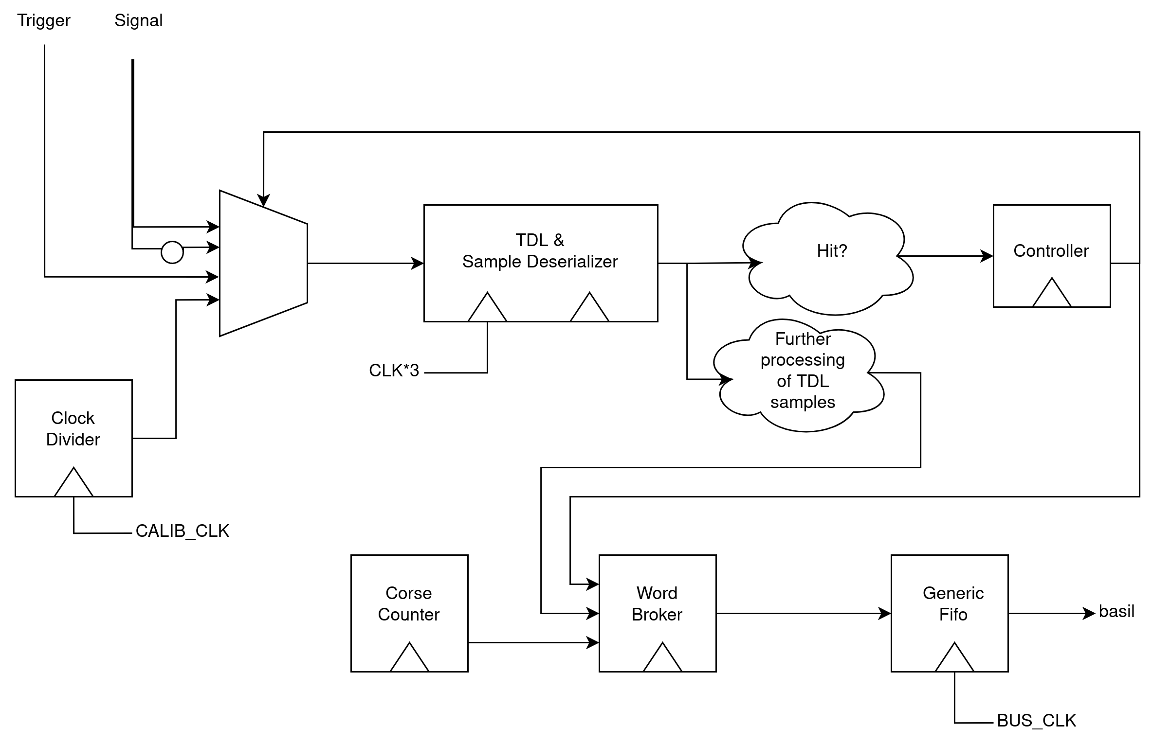
Tdl Tdc - Tapped Delay Line based Time to Digital Converter#
utils/3_stage_synchronizer.v
utils/flag_domain_crossing.v
utils/generic_fifo.v
utils/cdc_syncfifo.v
utils/clock_divider.v
30ps RMS accuracy
40ns shortest reliably detectable pulse length
400us dynamic range
Before every experiment, the Tdc should be calibrated, ideally after it had time running to warm up. This can be done as follows:
chip['TDL_TDC'].EN_CALIBRATION_MOD = 1
time.sleep(1)
chip['TDL_TDC'].EN_CALIBRATION_MOD = 0
This will cause the Tdc to write many CALIB words to the fifo. Subsequently any required configuration bits for the particular experiment may be set. During analysis the recorded
calibration stream is easily incorporated:
calib_data_indices = chip['TDL_TDC'].is_calib_word(collected_data)

if any(calib_data_indices) :
    calib_values = chip['TDL_TDC'].get_raw_tdl_values(np.array(collected_data[calib_data_indices]))
    chip['TDL_TDC'].set_calib_values(calib_values)
    logging.info("Calibration set using %s samples" % len(calib_values))
Optionally, you can view a histogram of the calibration using chip['TDL_TDC'].plot_calib_values(calib_values).
If measurements are made over a longer time span, recalibration might be necessary, however note that the above example lumps all the calibration(s) in
collected_datatogether.
The calibrated basil module can then be used the following way:
time_word_indices = chip['TDL_TDC'].is_time_word(collected_data)
time_data = collected_data[time_word_indices]
if any(calib_data_indices) :
        time_in_ns = chip['TDL_TDC'].tdc_word_to_time(time_data[0])
Under examples/tdc_bdaq you can find an example implementation of the module along side a sequence generator to generate test signals. The TDC uses the external Si570 oscillator while the signal generator uses the external Si550. The script generates pulses of varying trigger distance and creates a plot of the difference of measured and expected time values, alongside errorbars of the standard deviation.
Unit test/Example: test_SimTdl_Tlu.v test_SimTdl_Tlu.py
Name
Default
Description
DATA_IDENTIFIER
4’b0100
4-bit data identifier for TDC words.
Name
Size
Direction
Description
CLK480
1
input
480 MHz clock
CLK160
1
input
160 MHz clock
CALIB_CLK
1
input
Any clock that is uncorrelated. For example the ethernet clock
CLK125RX.tdc_in
1
input
input pulse which is digitized
trig_in
1
input
input trigger signal (distance between TRIG_IN and TDC_IN can be measured)
arm_tdc
1
input
enable TDC for single measurement
ext_en
1
input
enable TDC for a fixed time period
timestamp
16
input
timestamp counter from other modules (e.g. tlu module)
Name
Address
Bits
r/w
Default
Description
RESET
0
wo
reset
VERSION
0
[7:0]
ro
3
version
ENABLE
1
[0]
r/w
0
enable TDC module (*)
ENABLE_EXTERN
1
[1]
r/w
0
external enable (*)
EN_ARMING
1
[2]
r/w
0
enable arming (*)
EN_WRITE_TIMESTAMP
1
[3]
r/w
0
write timestamp to output data (see data format description )
EN_TRIGGER_DIST
1
[4]
r/w
0
write trigger distance to output data
EN_NO_WRITE_TRIG_ERR
1
[5]
r/w
0
NOT IMPLEMENTED
EN_INVERT_TDC
1
[6]
r/w
0
invert TDC input (*)
EN_INVERT_TRIGGER
1
[7]
r/w
0
invert trigger input (*)
EVENT_COUNTER
2
[31:0]
ro
event counter value (*)
LOST_DATA_COUNTER
6
[7:0]
ro
lost data counter (*)
TDL_MISS_COUNTER
7
[7:0]
ro
signal transistions not registered by delay line (*)
EN_CALIBRATION_MODE
8
[0]
ro
sample and write calibration data
The Tdc module uses a state machine to send various types of 32 bit data words, however the first seven bits always follow the same structure:
DATA IDENTIFIER (4 bit) |
WORD TYPE (3 bit) |
Data (25 bits) |
The three bit codes for the individual word types can be found in word_broker.v, but the basil driver can decode these without manual effort. The words containing the tdc information are in the following order:
[TRIGGERED] -> RISING -> FALLING -> [TIMESTAMP]
TRIGGERED is only sent if EN_TRIGGER_DIST, and TIMESTAMP only if EN_WRITE_TIMESTAMP is set. Note however, that this sequence can be interrupted and appear incomplete, for example if the module is reset during a measurement.
In the following, we list how the remaining 25 bits are allocated for the various words.
160 Mhz Counter (16 bits) |
480 Mhz Counter (2 bits) |
Delay Line (7 bits) |
This word comes after the FALLING word, but the Timestamp is actually sampled two 160Mhz clock cycles after a measurement has been started.
Timestamp (16 bits) |
0 (9 bits) |
If the Tdc is set for self-calibration using EN_CALIBRATION_MODE, it will repeatedly send this word.
0 (16 bits) |
480 Mhz Counter (2 bits) |
Delay Line (7 bits) |
If a reset is issued to the Tdc, either as a global bus reset or through basil, this word is sent. It might be useful for resetting a state machine decoding the words on the receiving end. The Timestamp included is sampled as soon as the reset signal has passed the clock domain crossing circuitry.
Timestamp (16 bits) |
0 (9 bits) |
The TDC is built around the delay line found in the Link jTDC which uses about 200 delay elements of which only every second is sampled. This is done because the bin size variance is very large so that if every tap is used, hardly more precision will be obtained. However, this relatively long delay line can be sampled with a lower rate without missing signals. Implementations using every tap usually use several delay lines of about 100 elements which are then sampled using different clock phases. One such implementation can be found in the Link master thesis of Benjamin Blase, which will also give interesting insights to TDC architecture considerations. The priority encoder of this TDC, i.e. the module converting the delay line thermometer code to binary, is based on his work.
In order to sample the delay elements at a high enough rate while still being able to process them, we use a 3x multisampling approach: There is a shift register shifting in the entire information of the delay line using the 3x clock and at every slow clock tick the contents of the shift register are copied for further processing in the slow clock domain. Only then do we detect signal transitions and convert the thermometer code to binary.
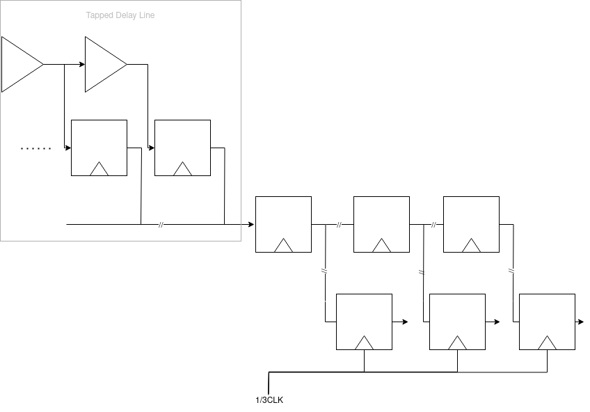
The most distinct design choice in this implementation is that it uses only a single delay line for measuring rising and falling edges of two inputs. As rising and falling edges propagate delay elements differently it makes sense to treat with distinct calibrations or even separate delay lines. To circumvent this additional space requirement and complexity, we use a multiplexer co-ordinating which input, in which polarity, gets seen by the delay elements. This induces a lower bound on width of pulses we can measure as this input multiplexer needs some time to switch between signals. To drive the multiplexer we use a simple state machine, which also drives the word output generation in the word_broker module.
Driver:
- class basil.HL.tdl_tdc.tdl_tdc(intf, conf)[source]#
TDC controller interface
- calib_sum = np.float64(92.0)#
- calib_vector = array([1., 1., 1., 1., 1., 1., 1., 1., 1., 1., 1., 1., 1., 1., 1., 1., 1., 1., 1., 1., 1., 1., 1., 1., 1., 1., 1., 1., 1., 1., 1., 1., 1., 1., 1., 1., 1., 1., 1., 1., 1., 1., 1., 1., 1., 1., 1., 1., 1., 1., 1., 1., 1., 1., 1., 1., 1., 1., 1., 1., 1., 1., 1., 1., 1., 1., 1., 1., 1., 1., 1., 1., 1., 1., 1., 1., 1., 1., 1., 1., 1., 1., 1., 1., 1., 1., 1., 1., 1., 1., 1., 1.])#
timestamp - Timestamp#
Simple timestamp recorder.
Unit test/Example: test_Timestamp.v test_Timestamp.py
- Pins:
Name
Size
Direction
Description
EXT_ENABLE
1
input
active high accept DI signal (synchronous to CLK)
CLK
1
input
module clock
DI
1
input
input signal
EXT_TIMESTAMP
64
input
external timestamp timestamp pulse
TIMESTAMP_OUT
64
output
- Registers:
Name
Address
Bits
r/w
Default
Description
EN
2
[0]
r/w
enable module
EXT_TIMESTMP
2
[1]
r/w
0
use external timestamp
EXT_ENABLE
2
[2]
r/w
0
enable external start
Driver:
bram_fifo - data FIFO (BRAM)#
Data FIFO implemented based on internal BRAM memory. Can be continuously pooled for data.
Driver:
- class basil.HL.bram_fifo.bram_fifo(intf, conf)[source]#
BRAM-backed FIFO controller.
The corresponding firmware module stores incoming 32-bit FIFO words in FPGA BRAM. The regular
base_addrconfiguration key addresses the control registers, whilebase_data_addrmust point to the 32-bit data window used byget_data().FIFO_SIZEreports the amount of buffered data in bytes. The driver rounds this down to complete 32-bit words before reading data.- property FIFO_INT_SIZE#
Get FIFO size in units of integers (32 bit).
Returns#
- fifo_sizeint
FIFO size in units of integers (32 bit).
- get_FIFO_INT_SIZE()[source]#
Get FIFO size in units of integers (32 bit).
Returns#
- fifo_sizeint
FIFO size in units of integers (32 bit).
- get_data()[source]#
Read all currently buffered complete 32-bit words.
The method reads
FIFO_SIZEtwice and uses the smaller value to avoid requesting more data while the FIFO size is changing. Data are read frombase_data_addrand returned as little-endian unsigned 32-bit integers.Returns#
- arraynumpy.ndarray
Array of unsigned 32-bit FIFO words.
sram_fifo - data FIFO (SRAM)#
Data FIFO implemented using external 16-bit SRAM memory. Incoming 32-bit FIFO words are buffered internally and written to SRAM as two 16-bit words. Data are read back from SRAM through the USB_READ / USB_DATA interface.
- Parameters:
Name
Default
Description
BASEADDR
16’h0000
Base address for the control register bus
HIGHADDR
16’h0000
High address for the control register bus
ABUSWIDTH
16
Address bus width
DEPTH
21’h10_0000
FIFO depth in 16-bit SRAM words
FIFO_ALMOST_FULL_THRESHOLD
95
Almost-full threshold in percent
FIFO_ALMOST_EMPTY_THRESHOLD
5
Almost-empty threshold in percent
- Pins:
Name
Size
Direction
Description
SRAM_A
20
output
External SRAM address bus
SRAM_IO
16
inout
External SRAM data bus
SRAM_BHE_B
1
output
SRAM upper-byte enable, active low
SRAM_BLE_B
1
output
SRAM lower-byte enable, active low
SRAM_CE1_B
1
output
SRAM chip enable, active low
SRAM_OE_B
1
output
SRAM output enable, active low
SRAM_WE_B
1
output
SRAM write enable, active low
USB_READ
1
input
Read strobe for the USB data output
USB_DATA
8
output
USB data output
FIFO_READ_NEXT_OUT
1
output
Request next 32-bit input FIFO word
FIFO_EMPTY_IN
1
input
Input FIFO empty flag
FIFO_DATA
32
input
Input FIFO data word
FIFO_NOT_EMPTY
1
output
SRAM FIFO contains data
FIFO_FULL
1
output
SRAM FIFO is full
FIFO_NEAR_FULL
1
output
SRAM FIFO crossed the almost-full threshold
FIFO_READ_ERROR
1
output
A read was attempted while the SRAM FIFO was empty
- Registers:
Name
Address
r/w
Description
RESET
0
wo
Soft reset on write to address
VERSION
0
ro
Module version
ALMOST_FULL_THRESHOLD
1
r/w
Almost-full threshold value
ALMOST_EMPTY_THRESHOLD
2
r/w
Almost-empty threshold value
READ_ERROR_COUNTER
3
ro
Read attempts while the SRAM FIFO is empty
FIFO_SIZE
4 - 7
ro
Stored FIFO data size in bytes
The FIFO_SIZE register is exposed as a 32-bit value by the Python driver. The firmware currently reports a 22-bit byte count and returns zero for the upper byte at address 7.
Driver:
- class basil.HL.sram_fifo.sram_fifo(intf, conf)[source]#
External-SRAM-backed FIFO controller.
The corresponding firmware module stores incoming 32-bit FIFO words in an external 16-bit SRAM. The regular
base_addrconfiguration key addresses the control registers.base_data_addrmust point to the transfer-layer data path used byget_data()to drain buffered FIFO words.FIFO_SIZEreports the amount of buffered data in bytes. The driver rounds this down to complete 32-bit words before reading data.- property FIFO_INT_SIZE#
Get FIFO size in units of integers (32 bit).
Returns#
- fifo_sizeint
FIFO size in units of integers (32 bit).
- get_FIFO_INT_SIZE()[source]#
Get FIFO size in units of integers (32 bit).
Returns#
- fifo_sizeint
FIFO size in units of integers (32 bit).
- get_data()[source]#
Read all currently buffered complete 32-bit words.
The method reads
FIFO_SIZEtwice and uses the smaller value to avoid requesting more data while the FIFO size is changing. Data are read frombase_data_addrand returned as little-endian unsigned 32-bit integers.Returns#
- arraynumpy.ndarray
Array of unsigned 32-bit FIFO words.
- get_fifo_int_size()[source]#
Deprecated Get FIFO size in units of integers (32 bit).
Returns#
- fifo_sizeint
FIFO size in units of integers (32 bit).
- get_fifo_size()[source]#
Deprecated Get FIFO size in units of bytes (8 bit).
Returns#
- fifo_sizeint
FIFO size in units of bytes (8 bit).
- get_read_error_counter()[source]#
Deprecated Get read error counter.
Returns#
- fifo_sizeint
Read error counter (read attempts when SRAM is empty).
gpac_adc_rx - ADC receiver (GPAC)#
Received data are propagated to FIFO data interface.
Driver:
m26_rx - MIMOSA26 data receiver#
Allows continuous data recording from MIMOSA26. Received data are propagated to FIFO data interface. Implements error monitoring.
Driver:
i2c - I2C peripheral interface#
Module implements master i2c peripheral interface.
Unit test/Example: test_SimI2c.v test_SimI2c.py
- Parameters:
Name
Default
Description
MEM_BYTES
16
Amount of memory (bytes) allocated for data (maximum single transfer in bytes)
- Pins:
Name
Size
Direction
Description
I2C_CLK
1
input
clock used for i2c transfers (internally devided by 4)
I2C_SDA
1
inout
SDA
I2C_SCL
1
inout
SCL
- Registers:
Name
Address
Bits
r/w
Default
Description
START
1
wo
start transfer on write to address
READY
1
[0]
ro
0
indicate transfer finish
NO_ACK
1
[1]
ro
0
status of previous transfer
SIZE
4 - 3
[15:0]
r/w
0
size of transfer (in bytes)
ADDR
2
[7:0]
r/w
0
i2c slave address
MEM_BYTES
7 - 6
[15:0]
ro
MEM_BYTES
size of memory (bytes)
DATA
8 to 8+MEM_BYTES-1
r/w
unknown
memory for data
Driver:
- class basil.HL.i2c.i2c(intf, conf)[source]#
Implement master i2c programming interface driver.
- property is_ready#
- Raises:
IOError – Transfer not acknowledged.
jtag - JTAG master#
Module implements master jtag peripheral interface. Supports simple internal loops.
Unit test/Example: test_SimJtagMaster.v test_SimJtagMaster.py
- Parameters:
Name
Default
Description
MEM_BYTES
16
Amount of meemory allocated for data (maximum single transfer in bytes)
- Pins:
Name
Size
Direction
Description
JTAG_CLK
1
input
clock used for SPI transfers
TCK
1
output
external clock (active only during transfers)
TDO
1
input
incoming data
TDI
1
output
outgoing data
TMS
1
output
jtag machine state control pin
SEN
1
output
active high during transfer
SLD
1
output
active high strobe indicating end of transfer
- Registers:
Name
Address
Bits
r/w
Default
Description
START
1
wo
start transfer on write to address
DONE
1
[0]
ro
0
indicate transfer finish
BIT_OUT
4 - 3
[15:0]
r/w
MEM_BYTES*8
set the size of transfer in bits
WAIT
8 - 5
[31:0]
r/w
4
waits after every transfer if REPEAT != 0
WORD_COUNT
10 - 9
[15:0]
r/w
1
number of word to be sent (1 word = BIT_OUT bit long)
JTAG COMMAND
12 - 11
[15:0]
r/w
0
JTAG command 0 = SCAN_IR, 1 = SCAN_DR
MEM_BYTES
15 - 14
[15:0]
ro
MEM_BYTES
byte size of memory
DATA_OUT
16 to 16+MEM_BYTES-1
r/w
unknown
memory for outgoing data
DATA_IN
16+MEM_BYTES to 16+2*MEM_BYTES-1
r/w
unknown
memory for incoming data
Driver:
uart - UART slave#
Provides UART to basil interface.
utils#
Various Verilog modules used by basil.
3_stage_synchronizer
bus_to_ip
cdc_pulse_sync
cdc_pulse_sync_cnt
cdc_syncfifo
CG_MOD_neg
CG_MOD_pos
clock_divider
ddr_des
fifo_32_to_8
flag_domain_crossing
flag_domain_crossing_ce
generic_fifo
IDDR
IDDR_s3
ODDR
ODDR_s3
pulse_gen_rising
RAMB16_S1_S2
RAMB16_S1_S9
rbcp_to_bus
reset_gen
simple_arbiter
three_stage_synchronizer_ce
Arduino firmware#
Arduino Firmware for Environment Readout (temperature, humidity/pressure)#
Arduino Nano firmware to read out NTCs via the 8 analog input pins A0 to A7 and the internal (multiplexed) ADC.
NTC inputs require a voltage divider configuration, supplied with the 3.3 V Arduino rail.The voltage drop over the NTC is the input to the analog pin. The conversion from ADC value to degree Celsius can take place in the firmware.
Additionally, a pure analog read out is possible for processing of humidity and pressure sensors.
Arduino Firmware for NTC Readout#
Arduino Nano firmware to read out NTCs via the 8 analog input pins A0 to A7 and the internal (multiplexed) ADC. The REF and 3V3 need to be connected on the Arduino. Each input requires a voltage divider configuration, supplied with the 3.3 V Arduino rail. The voltage drop over the NTC is the input to the analog pin. The conversion from ADC value to degree Celsius takes place in the firmware.
Arduino Firmware for SiLab Relay Board#
Simple firmware for Arduino to take commands on serial port via USB and switch DigitalIO pins on and off accordingly. So far, all pins get initialized as LOW outputs, because of compatibility with 8 channel relay card.
Arduino Firmware for I2C over Serial#
Arduino Nano firmware to write and read an I2C bus over the Arduinos serial interface. The lines reqired by I2C are GND, VCC(3v3 or 5V), SDA (A4) and SCL (A5). The firmware receives read/write commands over serial, accesses the I2C bus and answers the results over serial.